


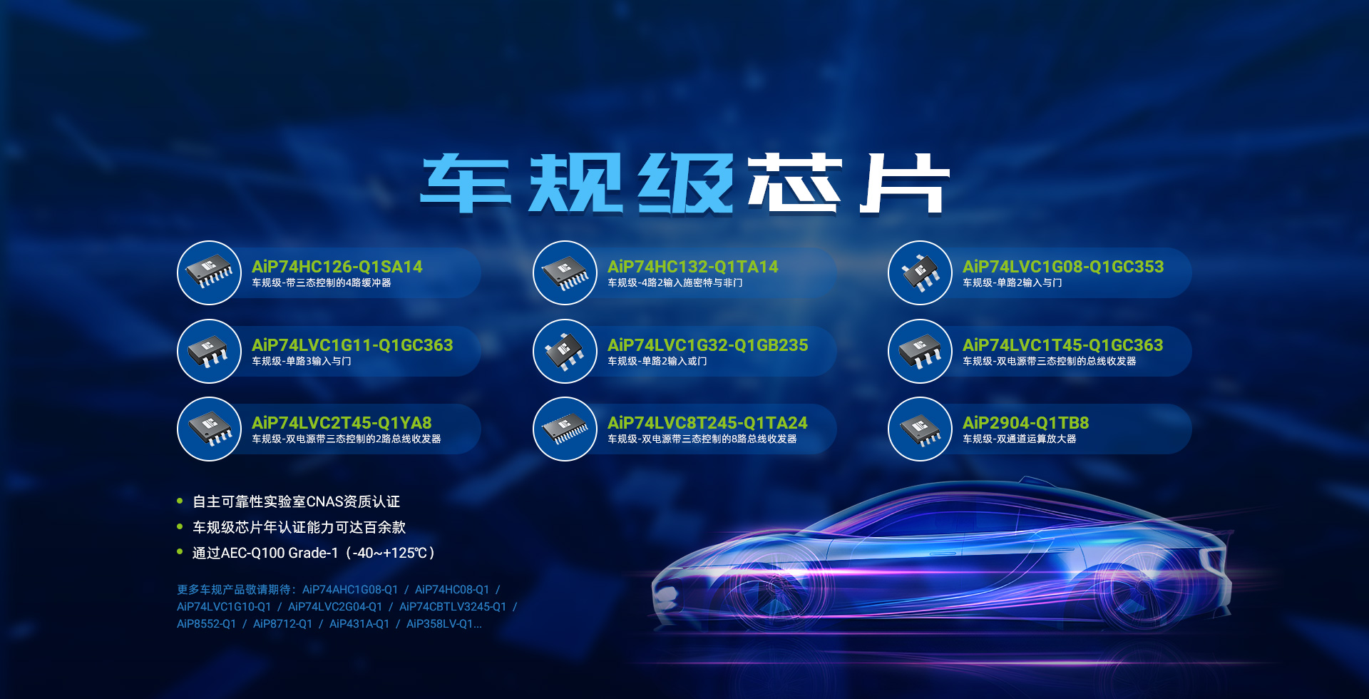
車(chē)規(guī)級(jí)芯片

顯示驅(qū)動(dòng)

MCU

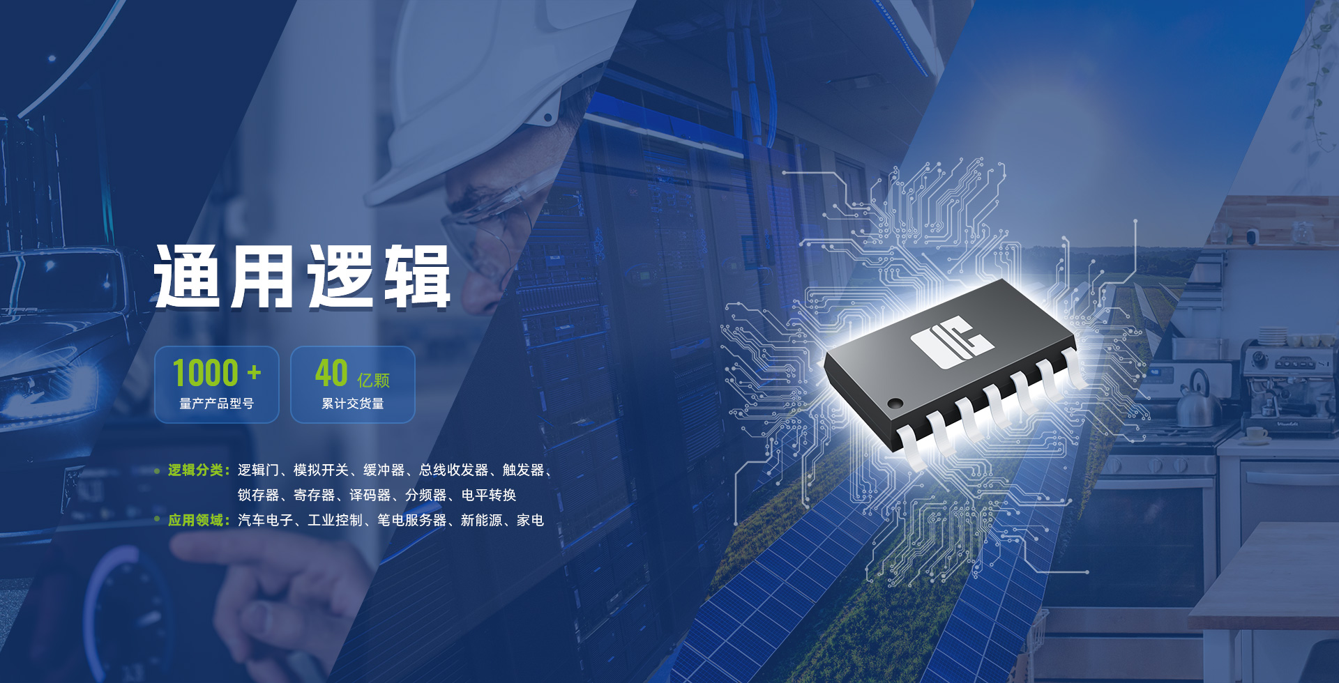
邏輯

信號(hào)鏈

電源

馬達(dá)&柵驅(qū)動(dòng)

音響


通信


-
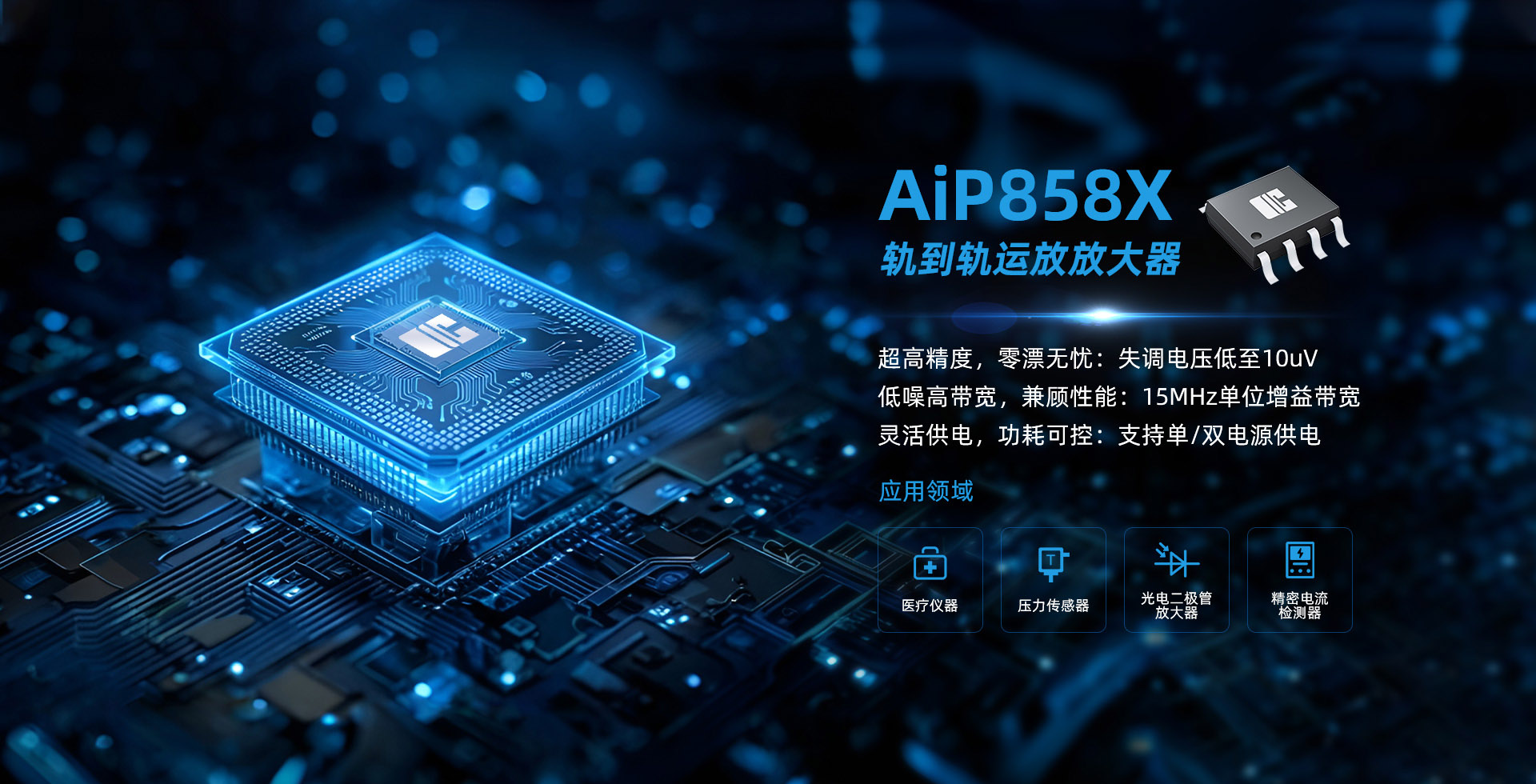
01AiP8931R▲-7MHz、40V 高擺率軌到軌輸出放大器
AiP8931R▲
AiP893XR 是一款 7MHz 高壓高擺率軌到軌輸出運(yùn)算放大器,工作電壓范圍為 3V~40V,單個(gè)放大器靜態(tài)電流 1mA,增益帶寬積 7MHz,提供寬輸入共模電壓范圍和軌到軌輸出,可用于電機(jī)控制與工業(yè)過(guò)程控制等。
了解詳情


-
02AiP5843-150V非隔離開(kāi)關(guān)電源轉(zhuǎn)換器
AiP5843
AiP5843 與 AiP5845 是用于開(kāi)關(guān)電源的 150V 高壓輸入開(kāi)關(guān)電源控制器,通過(guò)配合外圍無(wú)源器件將輸入電壓降至 5V 穩(wěn)定輸出。控制器設(shè)計(jì)具有 PFM 模式,可減小輕載開(kāi)關(guān)損耗,優(yōu)化轉(zhuǎn)換效率;具 有軟啟動(dòng)功能,能夠有效減小啟動(dòng)階段浪涌電流;具有頻率折返保護(hù),電感電流異常時(shí)降頻限流,防止電感電流飽和。AiP5843 與 AiP5845 同時(shí)集成了輸出欠壓保護(hù),輸出過(guò)載,過(guò)溫保護(hù)等各種保護(hù)功能。
了解詳情
-
03AiP74LV595-8-Bit Serial-In, Serial or Parallel-Out Shift Register with Output Latches; 3-State
AiP74LV595
The AiP74LV595 is an 8 stage serial shift register with a storage register and 3-state outputs. Both the shift and storage register have separate clocks. It is a low-voltage Si-gate CMOS device and is pin and functionally compatible with the AiP74HC595 and AiP74HCT595. Data is shifted on the positive-going transitions of the SHCP input. The data in the shift register is transferred to the storage register on a positive-going transition of the STCP input. If both clocks are connected together, the shift register will always be one clock pulse ahead of the storage register. The shift register has a serial input (DS) and a serial output (Q7S) for cascading the device. It is also provided with an asynchronous reset input MR— (active LOW) for all 8 shift register stages. The storage register has 8 parallel 3-state bus driver outputs. Data in the storage register appears at the output whenever the output enable input (OE—) is LOW.
了解詳情
-
04AiP8061*-500MHz軌到軌輸出運(yùn)算放大器
AiP8061*
AiP806X 是一款 500MHz 軌到軌輸出運(yùn)算放大器,電源電壓范圍為 2.5V~5.5V,單個(gè)放大器靜態(tài)電流 8.2mA,增益帶寬積為 200MHz,提供寬輸入共模電壓范圍和接近軌的輸出擺幅,具有快速的穩(wěn)定時(shí)間和低失真特性,可應(yīng)用在 ADC、DVD、濾波器、基帶等領(lǐng)域。
了解詳情
-
05AiP74AVCH8T245-8-Bit Dual Supply Translating ;Transceiver; 3-State
AiP74AVCH8T245
The AiP74AVCH8T245 is a 8-bit, dual supply transceiver that enables bidirectional level translation. It features two 8-bit input-output ports (An and Bn), a direction control input (DIR), a output enable input (OE) and dual supply pins (VCC(A) and VCC(B)). Both VCC(A) and VCC(B) can be supplied at any voltage between 0.8V and 3.6V making the device suitable for translating between any of the low voltage nodes (0.8V, 1.2V, 1.5V, 1.8V, 2.5V and 3.3V). Pins An, OE and DIR are referenced to VCC(A) and pins Bn are referenced to VCC(B). A HIGH on DIR allows transmission from An to Bn and a LOW on DIR allows transmission from Bn to An. The output enable input (OE) can be used to disable the outputs so the buses are effectively isolated. The AiP74AVCH8T245 has active bus hold circuitry which is provided to hold unused or floating data inputs at a valid logic level. This feature eliminates the need for external pull-up or pull-down resistors.
了解詳情


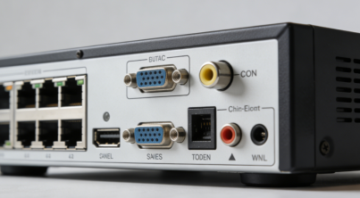


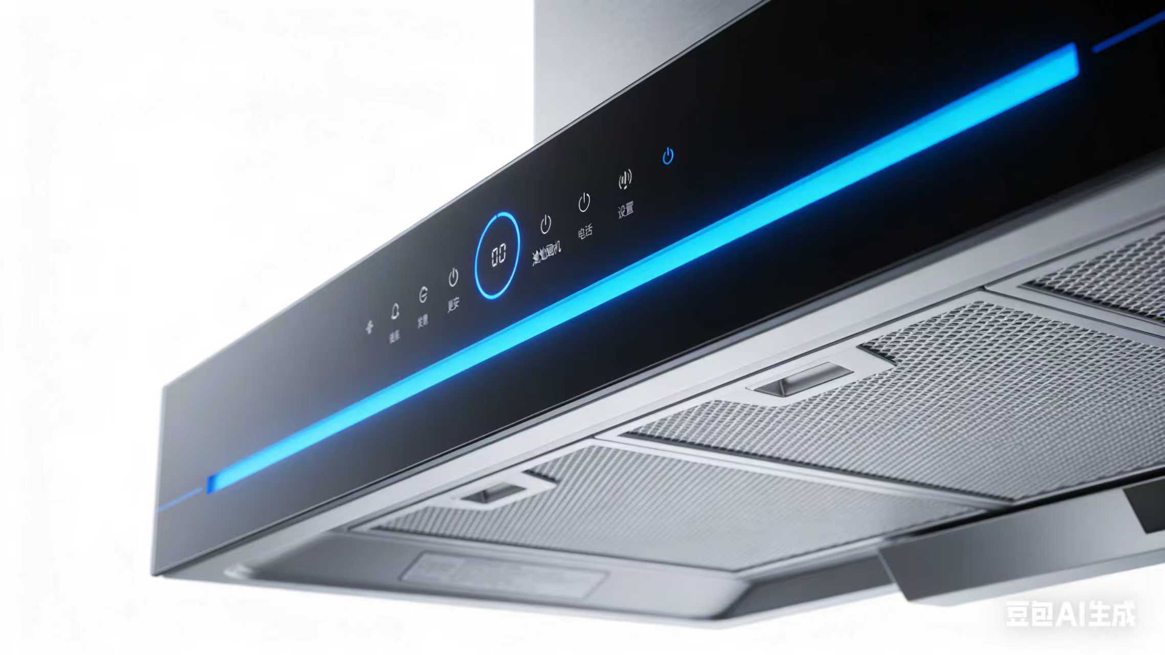


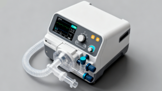


邏輯、信號(hào)鏈芯片
交叉檢索

咨詢(xún)熱線(xiàn)